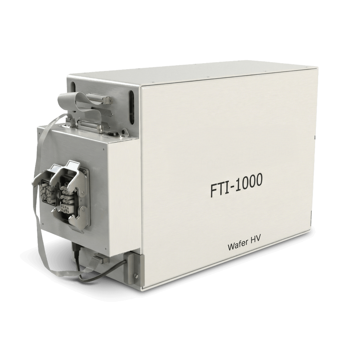
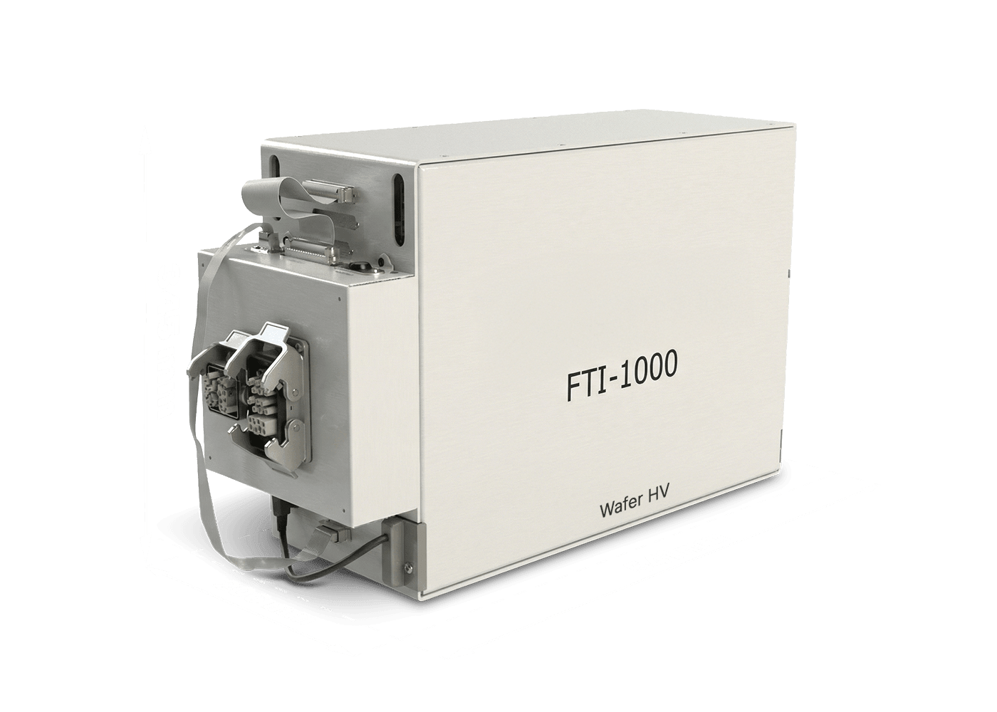
Wafer HV
Equipment
1 site HV Wafer Probe (6kV/200A)
The FTI‑1000 is designed for high‑coverage wafer‑level testing of semicondcutor devices and wide‑bandgap technologies, with strong suitability for multisite probe applications.
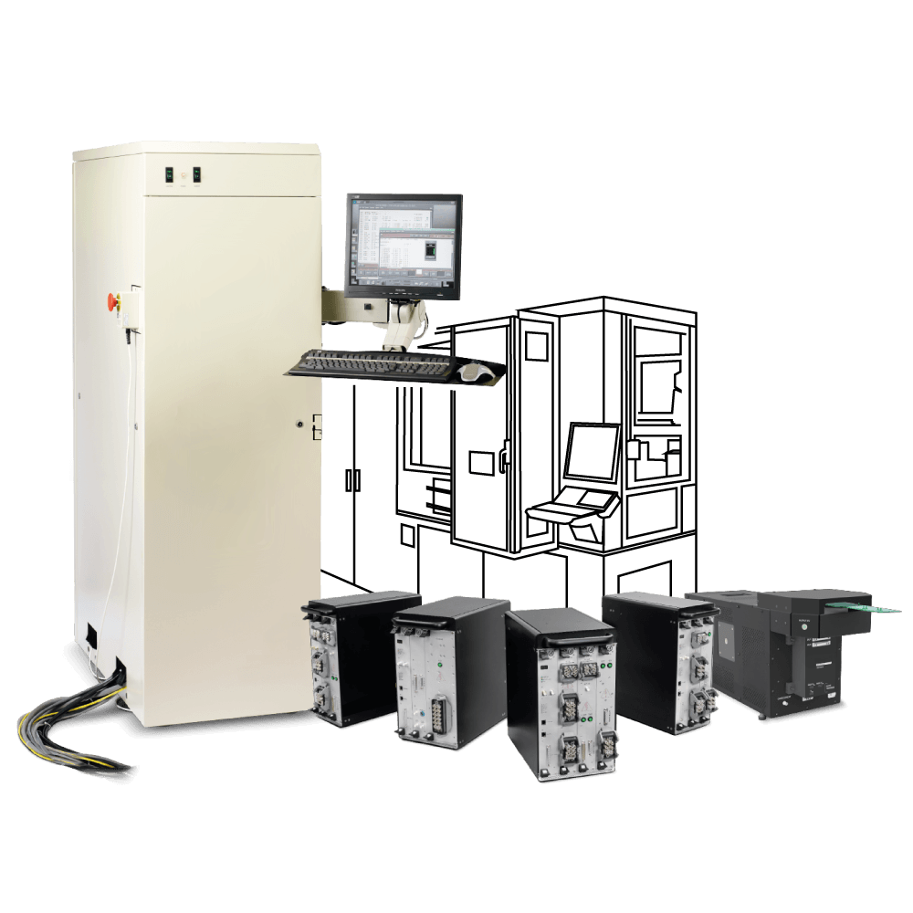
FTI‑1000 addresses the characterization needs of DC and AC parameters directly at wafer probe, supporting both engineering characterization and high‑volume wafer testing. Thanks to its modular Tester‑per‑Channel Board architecture, users can configure independent resources into a single flexible and scalable platform tailored to any wafer‑level test requirement.
Control is managed through FTI Studio, an intuitive graphical interface that simplifies probe‑card bring‑up, test‑program development, and debug, making the system equally accessible to Designers and Test Engineers.
Reasons Why
Product Presentation
The FTI‑1000 is a purpose‑built ATE system designed for high‑coverage wafer‑level testing of power discrete devices, wide‑bandgap components, and gate‑driver‑integrated power ICs. Suitable for both engineering characterization and high‑volume wafer sort, the system integrates independent DC and AC test resources capable of measuring all key MOSFET parameters, including DC characteristics, ΔVsd, inductive switching (UIL/UIS/CIS), gate charge, and gate resistance. Its modular Tester‑per‑Channel Board architecture, built on a USB‑based framework, enables straightforward system expansion and configuration flexibility for both single‑site and multisite probe applications.
With flexible resource partitioning and plug‑in options such as high‑voltage extensions, high‑current pulse modules, digitizers, and LCR‑based Rg measurement, the FTI‑1000 adapts seamlessly to a wide range of wafer‑level test requirements while maintaining a compact footprint. The architecture integrates cleanly with automated wafer probers and probe‑card interfaces—without being tied to any specific mechanical platform—making it equally effective for early‑stage device characterisation, process development, and high‑volume wafer‑sort operations.
FTI Studio software supports efficient test program development with tools such as waveform capture, automated data‑sheet generation, schmoo plotting, and AEC‑Q001 Rev. C PAT analysis. This combination of modular hardware, comprehensive test capability, and intuitive software makes the FTI‑1000 an ideal wafer‑test solution where flexibility, scalability, and high performance are essential, particularly in automotive, industrial, and wide‑bandgap power device sectors.
Wafer HV
Wafer MV
Dimensions
Power Supply: 345mm ⨯ 176mm ⨯ 103mm
Power Supply: 345mm ⨯ 176mm ⨯ 103mm
Digital
AC Source
Misc.
DC Source
More info