Services
Complete Test Services for Semiconductors
The Services division provides a full range of test services, from wafer sort and final production testing to characterization, qualification, reliability testing, and advanced failure and technology analysis, as well as ASIC design and design-for-testability (DFT) support to optimize device performance, testability, and time-to-market.
From ASIC Design to the Market
The Cosmic Services division provides a comprehensive portfolio of test services, supporting customers throughout the entire device lifecycle. Cosmic Services offers everything from customized test solution development, ASIC design with design-for-testability (DFT) support, to wafer sort and final production testing. On top of this, the division specializes in characterization and qualification testing in addition to burn-in and reliability testing. Cosmic ensures high-quality standards and fast execution for device troubleshooting projects ensured by advanced failure & technology analysis capabilities which enable precise identification of device failures through sophisticated failure analysis techniques, thereby supporting continuous improvement and product optimization processes.

Cosmic supports customers with:
- Outsourced Design Service
- IP Blocks Design/Portfolio
- Full ASIC (Application-Specific Integrated Circuit) / ASSP (Application specific standard product) Design.
During design stage, COSMIC can support on Design for Testability (DFT).

Cosmic offers full supply chain management through its qualified partner network of wafer foundries and assembly houses, acting as a single point of contact for customers.

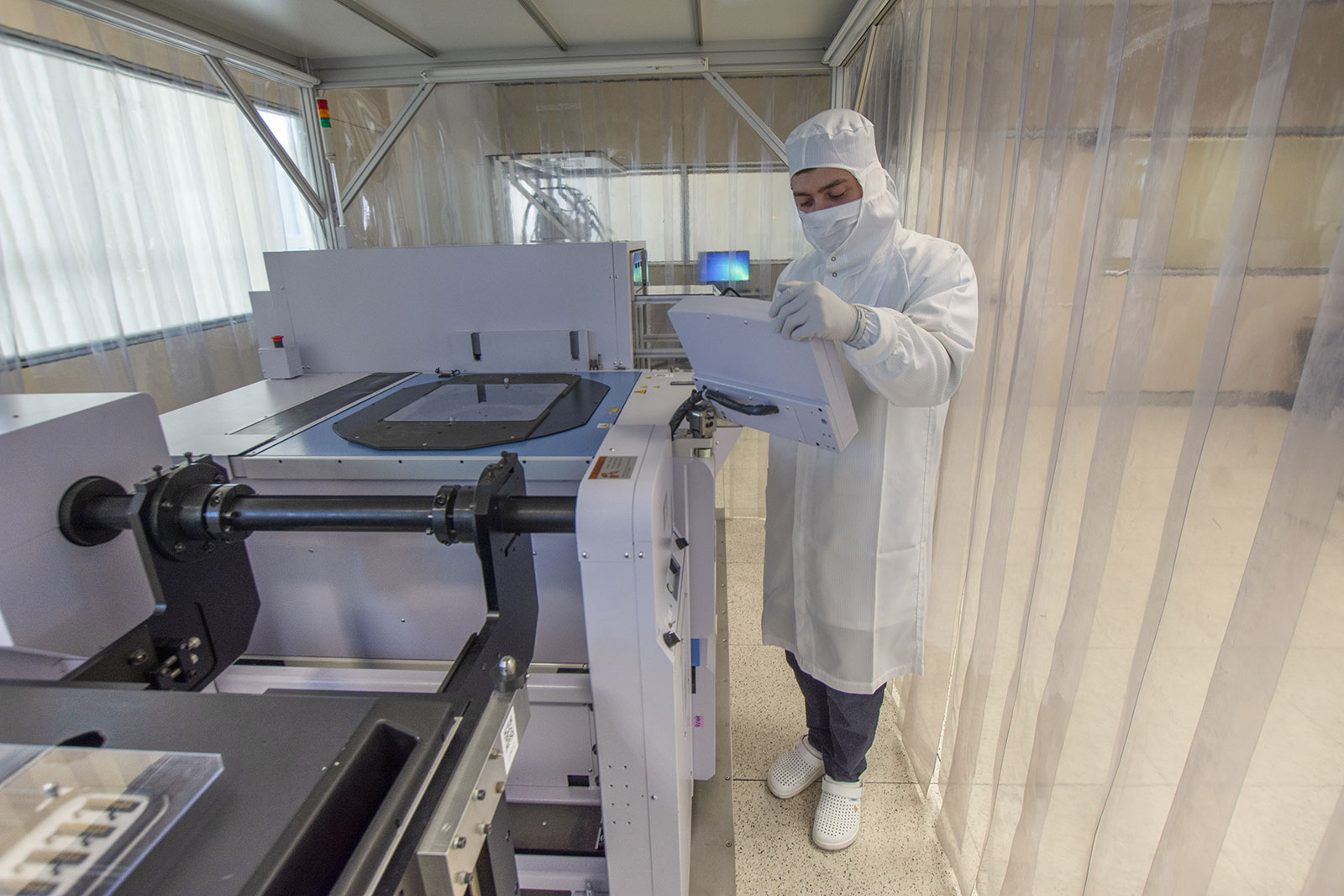
Cosmic develops tailored hardware and software test solutions, enabling efficient and reliable semiconductor production test.
Activities include:
- In-house design and manufacturing of load boards
- In-house design and manufacturing of probe cards
- Test program development enabling production tests such as scan, functional, power consumption and performance measurements
- Debugging, validation and release of production-ready test programs
This approach ensures robust, high quality production testing.

Prior to mass production release, electrical device characterization is performed during wafer and final test phases. These tests verify whether the device has been correctly designed, evaluate the impact of process parameters on its operation, and assess performance under varying environmental conditions.
Typical characterization activities include:
- Process, Voltage and Temperature (PVT) corner analysis
- Electrical performance validation

According to the product application and market requirements, a suitable package is selected or designed (e.g., QFN, BGA, WLCSP and others). After wafer testing, known good die are assembled in the selected package prior to the final production test stage.

Qualification and reliability testing are essential to ensure long-term device reliability and to prevent catastrophic failures at later stages of the product lifecycle. Industry-recognized qualification flows are applied to demonstrate compliance with application-specific standards, particularly for devices used in safety-critical environments.
Typical regulated markets include Automotive (AEC-Q, AQG 324), High-Reliability (MIL, ESCC) and other industrial applications.
Main qualification categories include:
- Lifetime & reliability tests
- Environmental stress tests
- Mechanical stress tests
- ESD and Latch-up
Cosmic supports customers with complete qualification runs according to applicable industry standards.

During high-volume production, Cosmic applies its engineering know-how and experience to continuously optimize key production parameters such as test parallelism, test time and production yield.
Through best-practice methodologies, Cosmic supports customers in achieving efficient and cost-effective high-volume semiconductor production.


Cosmic supports customers with advanced failure and technology analysis to identify root causes and prevent long-term reliability issues. Our experts not only help to detect failures but also work closely with customers to understand their origin and implement corrective actions.
Typical analysis areas include:
- Field return analysis
- Counterfeit product investigation
- PCB and soldering process issues
- Contamination and material defects
- Electrical and physical failure analysis
This consultation-driven approach helps prevent product issues and ensures long-term reliability.
Why Cosmic Services
Global Test Floors
full-service European test house with a global footprint in Europe and Asia, offering customers local engineering support and cost-effective volume production testing while enhancing supply chain resilience and operational efficiency.

Fully equipped
clean room test floors featuring state-of-the-art industry-standard automated test equipment. Our engineering teams offer extensive expertise in a broad range of world-class ATE platforms, ensuring reliable and advanced semiconductor testing capabilities.

Multidisciplinary engineering teams
across all sites support customers in developing complete test solutions – from test program development to production support and continuous optimization, in compliance with internationally recognized certified standards.

Customized production solutions
support customers throughout the full development cycle – from initial concept and engineering sample testing through qualification to high-volume mass production. Cosmic provides complete supply chain management, ensuring full traceability, reliable timelines, and minimized risks while optimizing logistics with the help of external suppliers.

Over 50 years of engineering excellence
delivering high-quality solutions and supply chain services to a broad range of market requirements from consumer to Hi-Rel in full compliance with applicable industry standards and supporting the most stringent customer and high-reliability requirements.

24/7 production test capability
across our global test floors, enabling efficient high-volume operations and ensuring uninterrupted production.

Gallery
Contact Us
FAQ
Semiconductor Test Services encompass the entire lifecycle of testing validation activities performed on an Integrated Circuit (IC) or Application Specific Integrated Circuit (ASIC). These services are critical because they ensure the device meets all electrical, functional, and reliability specifications before mass production and use in end applications (especially in safety-critical sectors like Automotive or Aerospace). They include everything from early Design for Testability (DFT) to final Production Test and Failure Analysis (Failure Analysis).
We become an all-in-one partner solution starting from the ASIC Design phase by applying Design for Testability (DFT) principles. This proactive involvement ensures that the circuit is inherently testable, which is vital for:
- Maximizing fault coverage (the percentage of possible defects that can be detected).
- Reducing the complexity and cost of the subsequent test program development.
- Optimizing the overall time to market.
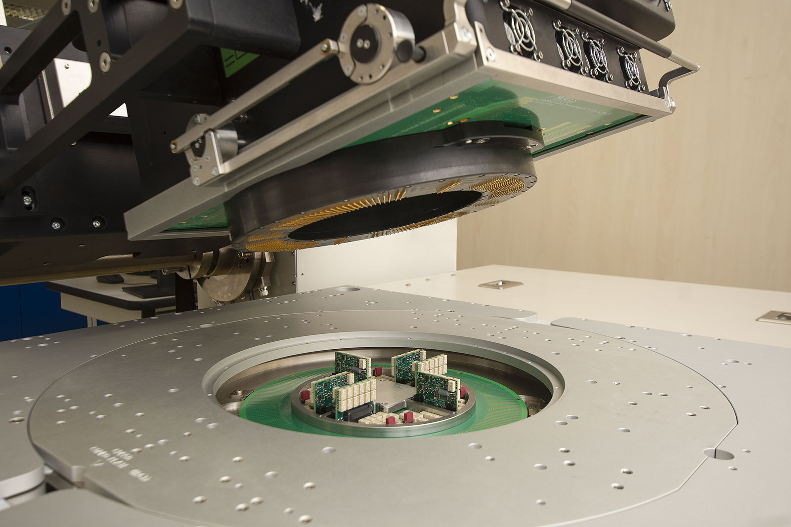
- Characterization Test (on wafer and on packaged devices): This phase performs in-depth electrical functional measurements to determine if the device has been designed correctly and how its performance varies across different conditions (e.g., PVT – Process, Voltage, Temperature). It is diagnostic and essential for design validation.
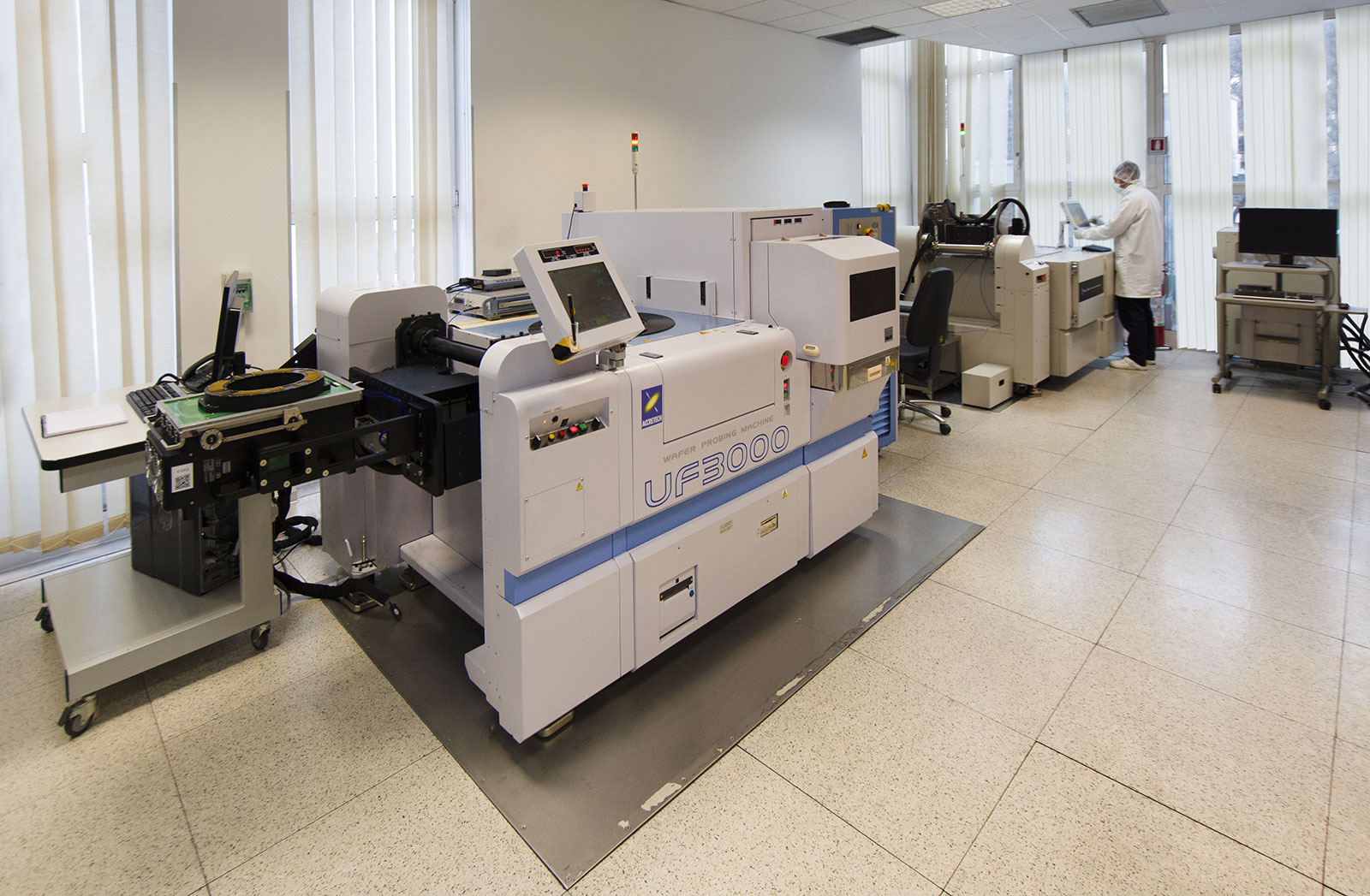
- Production Test (Wafer Sort – WS / Final Test – FT): This is the high-volume, pass/fail screening performed to ensure every device delivered meets specifications. The focus here is on efficiency, Test Time Reduction, and maximizing Production Yield.
Yes. We specialize in the in-house development and manufacturing of complete custom test solutions, including the Test Program (Software) and the necessary hardware, such as Probe Cards and Load Boards (or socket boards). This tailored approach ensures maximum accuracy and efficiency for your specific device under test (DUT).